Digital Timing Basics for VLSI Interview & SoC Design

Why take this course?
🚀 Master Digital Timing in VLSI Design with Learnin28days Academy's Expert-Led Course! 🎓
Course Title: Digital Timing Basics for VLSI Interview & SoC Design
Headline: A VLSI Course on Timing Concepts for Physical Design (Static Timing Analysis - STA), RTL & Circuit Design
Course Overview:
Learnin28days Academy presents an engaging and comprehensive online course designed specifically for VLSI students and professionals. This course is a must-take for anyone working in the fields of Physical Design / Front-end (RTL) Design / Verification / Circuit Design. It focuses on the fundamental understanding of digital timing basics that are indispensable for high-performance SoC design.
🎢 Key Learning Points:
-
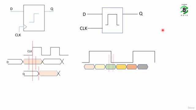
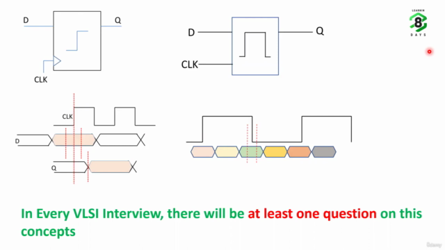
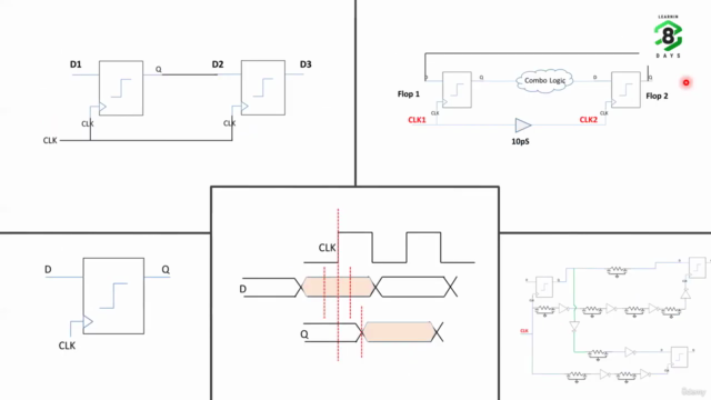
Comprehensive Understanding of Flops, Latches, and Logic Gates Timings: Gain a deep insight into the critical timing aspects of flip-flops, latches, and logic gates, including Set-up time, Hold-time, and Clock to Q delay.
-
Clock Skew and Timing Margins: Learn how to calculate set-up and hold margins and understand the impact of clock skew on Static Timing Analysis (STA).
-
Latency Minimization Techniques: Discover strategies for minimizing latency in your designs, a crucial aspect of Physical Design.
-
Industry Best Practices: Benefit from real-world insights shared by industry experts who have worked at top companies like Texas Instruments, AMD, Intel, Qualcomm, Rambus, Samsung, etc.
Why This Course?
-
Industry Relevant: Designed with input from leading professionals in the field, ensuring the content is up-to-date and relevant to current industry standards.
-
Career Enhancement: Ideal for VLSI aspirants preparing for interviews or competitive exams such as GATE.
-
Hands-On Learning: Each concept is followed by practical examples, enabling a deep understanding of the material covered.
-
Interview Preparation Focus: This course is perfect for VLSI interview preparation, providing a solid foundation in digital timing and its practical application.
Course Highlights:
-
Flop and Latch Operation: Understand how these elements function within a digital circuit.
-
Buffer Design and Usage: Learn the role of buffers in overcoming design challenges.
-
Clock Skew Management: Gain skills to analyze and manage clock skew effectively.
-
Timing Margin Analysis: Master the computation of set-up and hold margins to ensure reliable timing performance.
-
Cycle Path Analysis: Learn how to perform cycle path analysis for critical paths in your design.
-
Physical vs Digital Implementation: Understand the differences between digital design concepts and their physical implementation.
-
Identifying and Resolving Violations: Learn how to identify timing violations and effective strategies to fix them.
-
Latency Minimization: Discover techniques to minimize latency in your SoC designs.
-
Clock-Gating Techniques: Explore methods for efficient power management through clock-gating.
-
Frequency-Voltage Curve (FVC) Understanding: Learn how the FVC affects the performance and power characteristics of SoCs.
All the best as you embark on your VLSI journey with this comprehensive course! 🌟 Enroll now and take a significant step towards mastering digital timing in VLSI design.
Course Gallery


Loading charts...