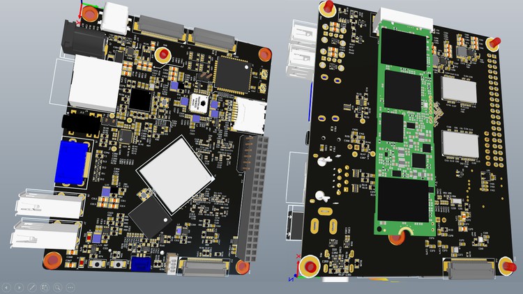
Advanced Hardware and PCB Design Masterclass 2022 -EsteemPCB

Why take this course?
🌟 Advanced Hardware Design Course Part-1: RK3399 COB (LPDDR4 SDRAM, WIFI/BT, EMMC, PMIC, 260 Pin DDR4 SoM) 🌟
Course Headline: Advanced Hardware Design Course Part-1 RK3399 COB
Introduction to the Course:
Hey there, Future Hardware Guru! This is the course for you if you're ready to dive deep into the world of advanced hardware design. With a focus on the Rockchip RK3399 Cortex-A53 processor, this 13-section masterclass will take you through every step of designing a sophisticated System on Module (SoM) with LPDDR4 SDRAM, WIFI/BT, EMMC, and more. By the end of this course, you'll be equipped to design any processor board without relying on simulation models or third-party tools. Let's embark on this exciting journey together!
What You Will Learn:
Section 1: Requirement Sheet and Processor Datasheet
- Understanding the RK3399 processor requirements and specifications in detail.
Section 2: SDRAM Selection and Schematic Design
- Choosing the right SDRAM (SDR/DDRX/LPDDRX) for your project and designing its schematic from the datasheet.
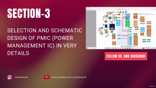
Section 3: Power Management IC (PMIC) Selection and Schematic Design
- Selecting a PMIC that fits your SoM's needs and designing its schematic with precision.
Section 4: EMMC Chip Selection, Pin Mapping, and Schematic Design
- Picking the right EMMC chip and integrating it into your SoM design.
Section 5: WIFI/BT Module Selection and Schematic Design
- Selecting certified WIFI/BT modules and designing their schematic, considering regulatory requirements like FCC, CE, etc.
Section 6: External LDO/DC-DC/Buck-Boost Design
- Understanding and implementing external power solutions for your SoM.
Section 7: Schematic Design of RK3399 with Impedance Planning
- Designing the schematic for the RK3399 processor, including impedance planning using net classes.
Section 8-10: Layer Stackup and Components Placement Planning
- Detailed guidance on selecting the layer stackup (4/6/8/12L) and executing components placement planning in three distinct stages.
Section 11-13: Layout Design, High-Speed Design Rules, and Optimization
- Creating a detailed layout plan, following high-speed design rules, and optimizing your design for performance and reliability.
Key Schematic Blocks Covered:
- Project Block Diagram
- Power Budget Block Diagram
- Power Supply Schematic for RK3399
- PMUIO Schematic Block of RK3399
- EMMC/PCIe/ADC Schematic for RK3399
- EDP/MIPI-DSI/HDMI Schematic for RK3399
- Type-C/USB3.0/USB2.0 Hosts Schematic for RK3399
- MIPI-CSI/GPIOs/I2C Schematic for RK3399
- And more!
Pre-Schematic Design and Basic Blocks:
- Understanding Pre-Schematic Design with Block Diagrams and Power Budgeting.
- Selecting the right Layer Stack-up for your PCB.
- Implementing different Grounding Techniques effectively.
- Analyzing the Power Distribution Network (PDN) of your PCB.
- Working with Ferrite Beads, ESD Diodes, and Magnetic Applications.
- Planning Placement and Layout using simple tools like Microsoft Paint.
Why Take This Course?
Upon completion, you'll have the skills to design a complex processor board without any reliance on simulation models or third-party support. This course is your stepping stone to becoming an expert in hardware design, with practical knowledge that you can apply directly to real-world projects. 🚀
Enroll now and take the first step towards mastering advanced hardware design! Let's unlock the potential of processor boards together. 🛠️💡
Course Gallery


Loading charts...